


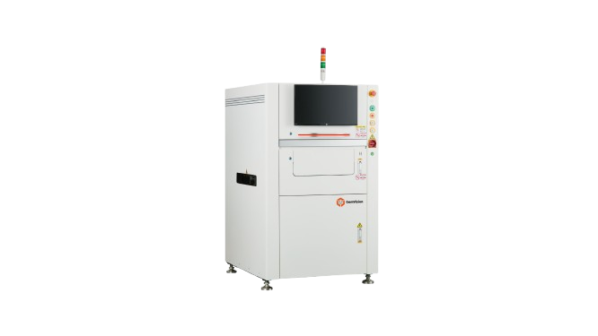
GA510S
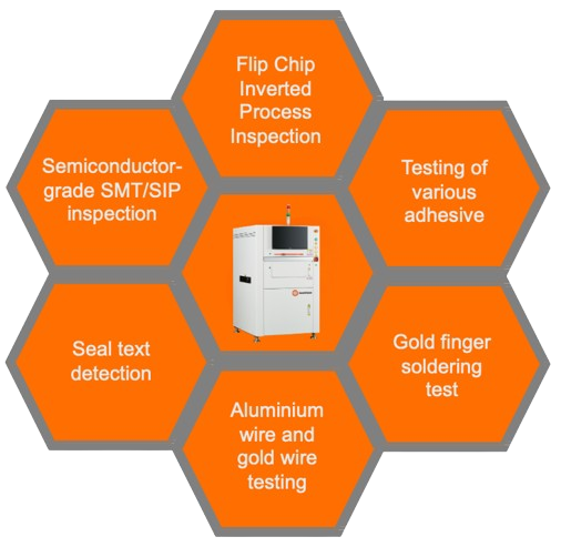
Semiconductor-grade SMT/SIP Inspection
Flip Chip Inverted Process Inspection
Testing of Various Adhesive
Gold Finger Soldering Test
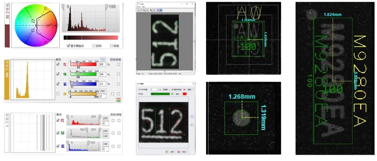
Seal Text Detection
Aluminium Wire and Gold Wire Testing
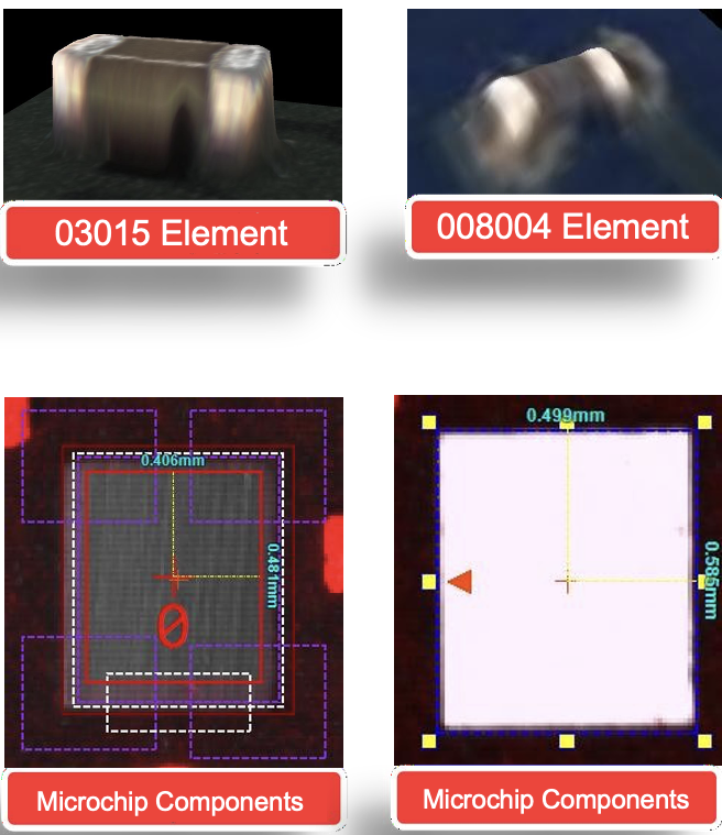
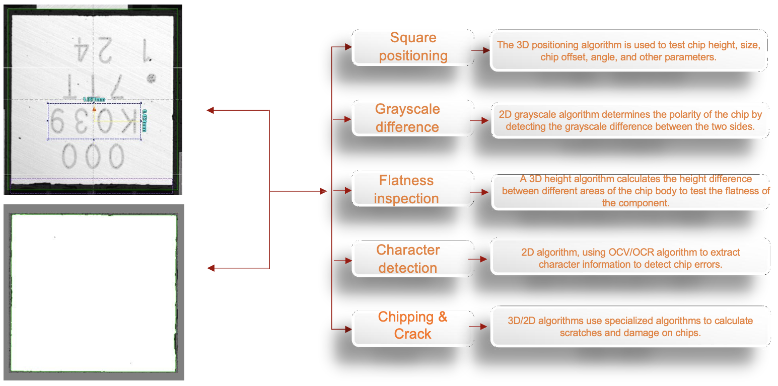
Square positioning - The 3D positioning algorithm is used to test component height, component size, component offset angle, and other parameters.
Colour Analysis - 2D colour algorithms test for component defects by extracting grayscale values of the three primary colours.
Solder Joint Inspection - A 3D+2D solder joint algorithm is used to test soldering effectiveness by measuring solder joint ramp height and solder joint colour.
Flatness Inspection - A 3D height algorithm measures the flatness of a component by calculating the height differences between different areas of the component body.
Algorithm Analysis for CHIP-type Microdevice Detection
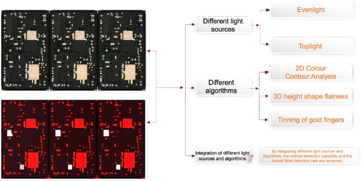
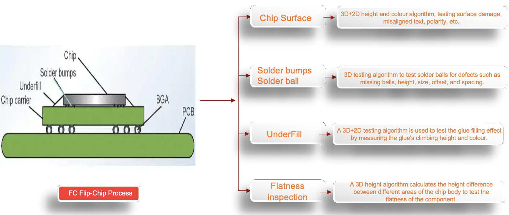
FC Component Detection Algorithm Analysis
DIE/Chip Detection Algorithm Analysis
Analysis of Chip Damage Detection Algorithm
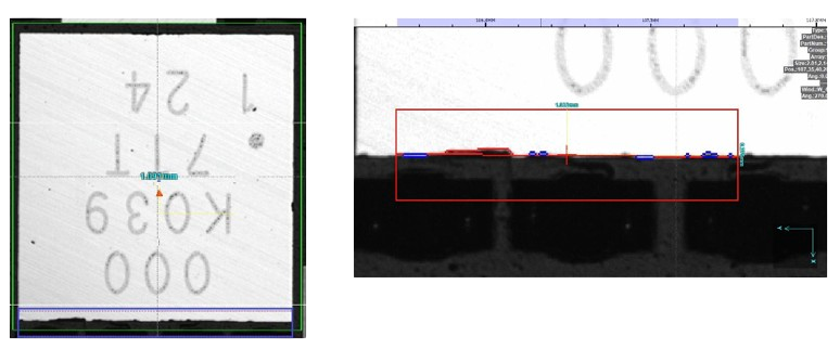
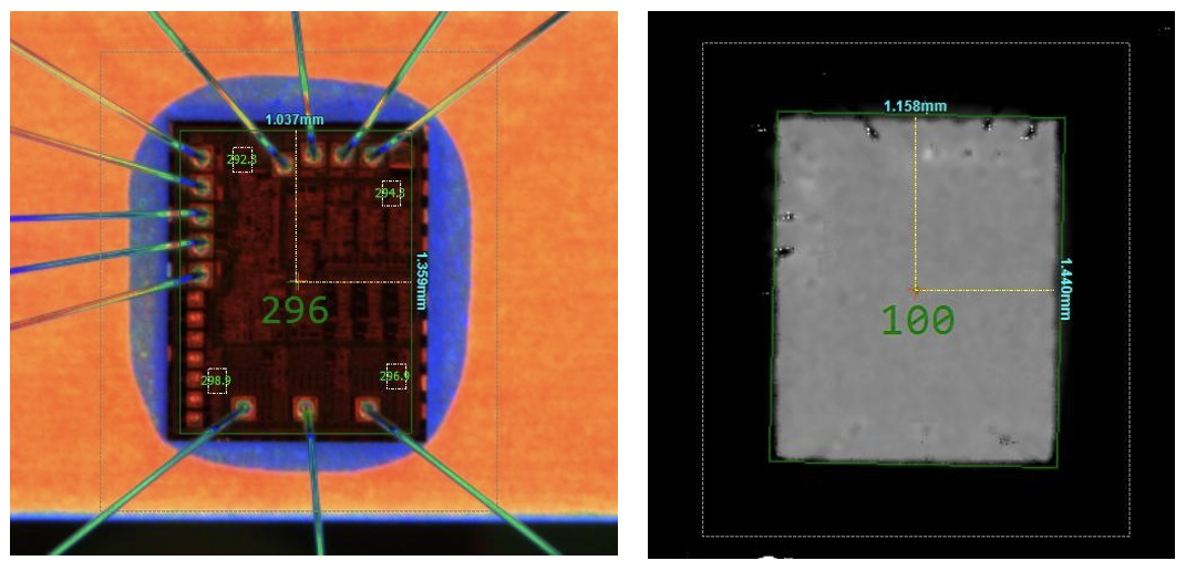
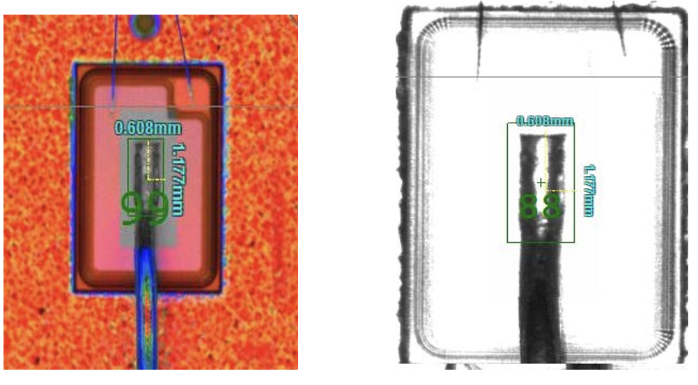
Line positioning - The 2D grayscale algorithm calculates the height and width of the maximum area by detecting the maximum area of the gaps on both sides of a straight line.
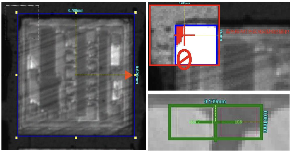
Analysis of Chipping Damage Detection Algorithms: 2D/3D Detection Algorithms
Right angle detection - 2D & 3D grayscale algorithms detect the area of right-angle defects by calculating the angle between two lines.
Detection of adhesives containing fluorescent agents
Analysis of Fluorescent Agent Glue Detection Algorithm -- 2D Colour Analysis
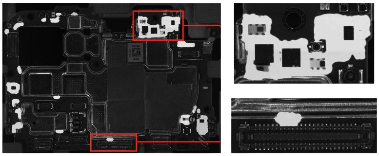
The 2D colour analysis algorithm, using a special light source, can clearly distinguish the glue application area. Then, the colour analysis algorithm calculates the glue area and detects defects such as insufficient glue or glue overflow.
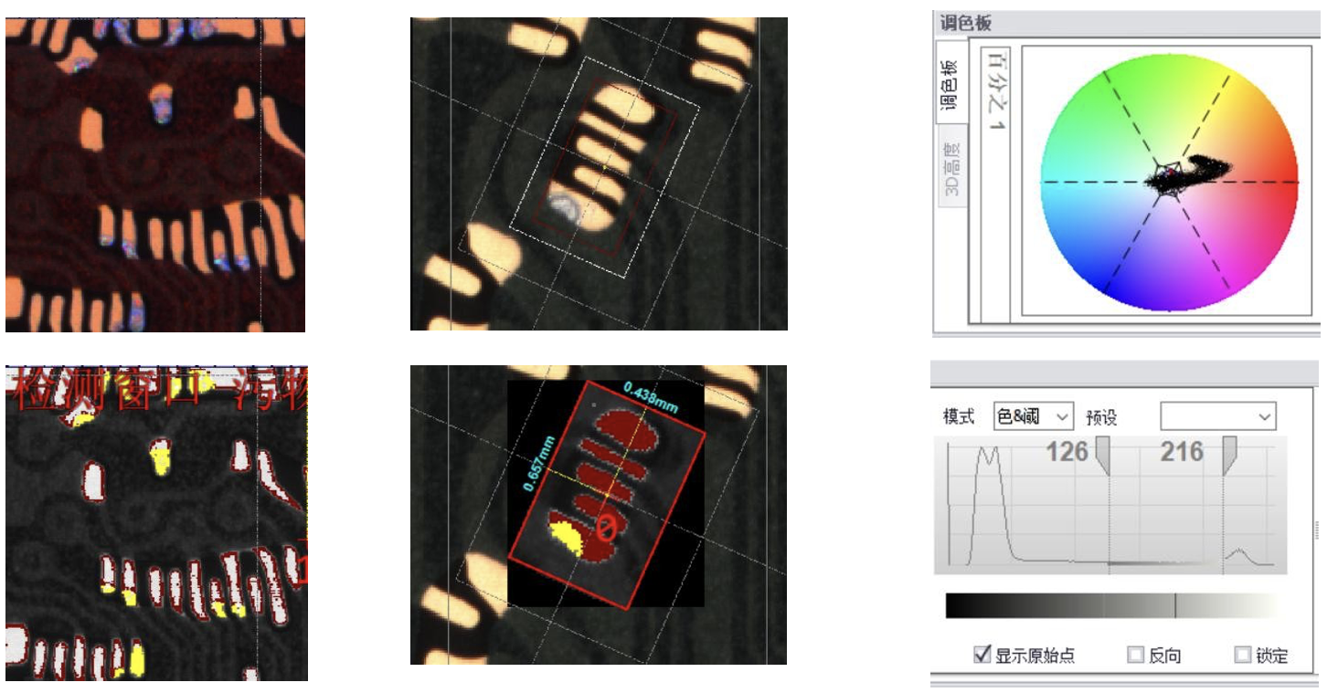
Analysis of Solder Adhesion Detection Algorithm for Gold Fingers - Wire Bonding Solder Joints
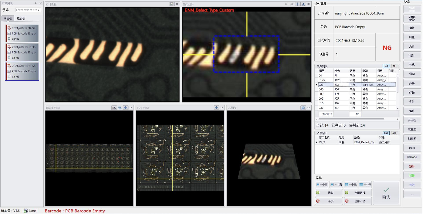
Gold finger soldering test RS service station fault confirmation interface
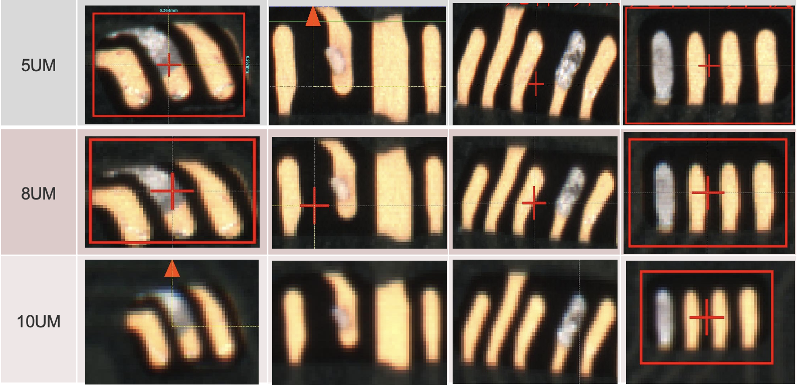
Detection of stamp text after moulding
Gem Vision AOI employs diverse image computation schemes, including Optical Character Verification (OCV), Optical Character Recognition (OCR), and Image & Color Matching algorithms. The programming steps are simple and clear, with well-defined and consistent parameters.
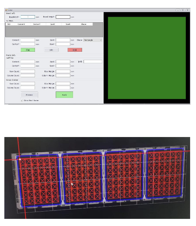
Overall framework import solution (Support Automatic Import of framework files and manual programming)
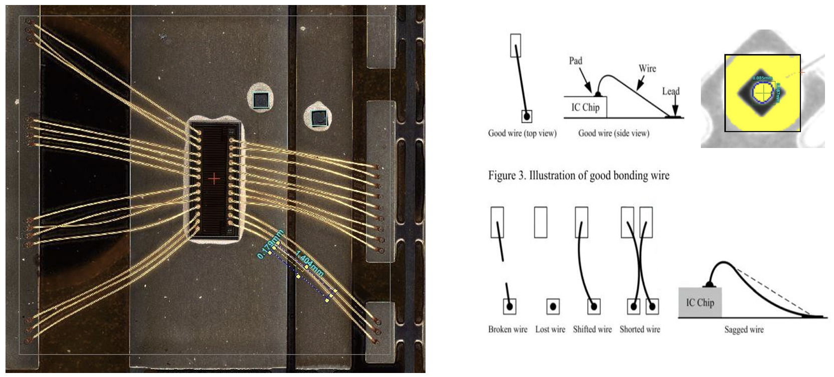
Analysis of Wire Bonding Detection Algorithms
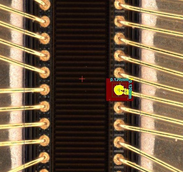
Analysis of Wire Bonding Detection Algorithms - Golden Ball
3D Moulding Inspection for Wire Bonding
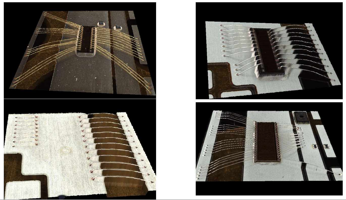
Analysis of Wire Bonding Detection Algorithms
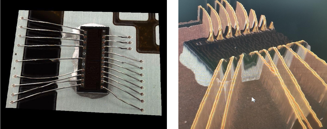
Chip Inspection Algorithm - Chips Positioning, Flatness Detection, Silver Paste Detection
IGBT Aluminium Wire Testing
AI Algorithms automatically recognises lines, eliminating the need for manual drawings of outlines.
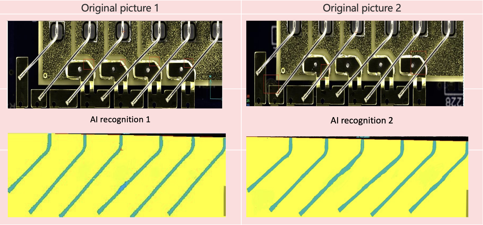
It can test defects such as the shape, size and offset of bonding points
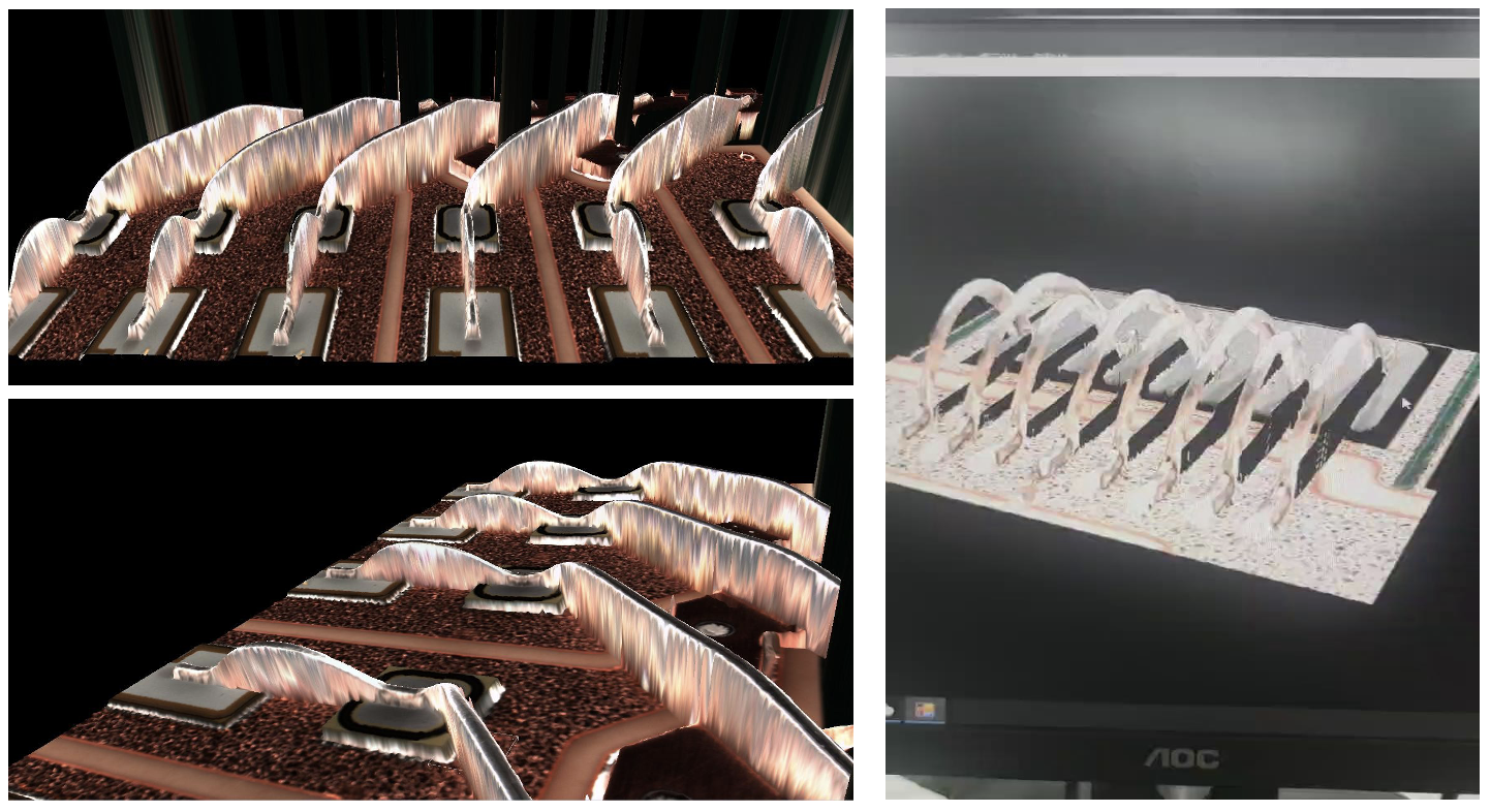
Aluminium Wire Height Detection Algorithm - 3D Line testing
| Technology Platform | Semiconductor Type A |
|---|---|
| Series | GA |
| Model | GA510S |
| Measurement Principle | 3D white light PSLM PMP (Programmable Spatial Light Modulation, Phase Measurement Profilometry) |
| Measurements | Defective Component, Defective Chip, Defective Golden Finger, Poor Glue Quantity, Defective Seal after Plastic Sealing |
| Detection of Non-Performing Types | Defective components: (Missing parts, offset, rotation, three-dimensional polarity, upside down, OCV, side standing, tombstone, poor soldering, etc.) UV/UF glue defective: (Less glue, more glue, size, area, shape, etc.) Chip Defects: (Missing chip, Offset, Rotation, Chipping Crack, Flatness, Contamination, etc.) Poor threads: (Missing threads, broken threads, lapped threads, high threads, abnormal bonding points, etc.) |
| Camera Pixel | 12M/19M/21M/25M |
| Lens Resolution | 3μm-15μm |
| FOV Size | 20mm X 15mm (12M 5μm) optional: 1.8μm, 3.1μm, 7μm, 10μm Resolution and 1600W, 2000W Camera |
| Accuracy | XY (Resolution): 10μm (5μm Optional) |
| Repeatability | Height:≤1μm (4 Sigma); volume/area: ≤1% (4 Sigma) |
| Gage R&R | <10% |
| Inspection Speed | 0.3 sec/FOV (2D Mode), 0.6 sec/FOV (3D Mode) |
| Quantity of Inspection Head | 4 |
| 2D Light Source | Multi-angle, Multi-zone, Three colour 2D Light Source (RGB+W) |
| Mark-point Detection Time | 0.3sec/piece |
| Maximum Measuring Head | 10mm |
| Maximum Height of Element on PCB | 10mm |
| Maximum Measuring Height of PCB Warp | ±5mm (15μm) |
| Minimum Element | 008004 |
| Maximum Loading PCB Size(X*Y) | 450mm x 450mm |
| Conveyor Setup | Front fixed orbit, Second orbit moving |
| Loader & Unloader | With a direct transfer station interface, ready for the optional installation of a high-capacity magazine auto-loader/unloader capable of simultaneous handling of up to four magazines |
| Bar-code Read | Support 1D/2D Barcode Reading |
| Traceability System | Support automatic generation of mapping and upload SECS/GEM |
| Maximum Jig Dimension | 450mmX450mm |
| PCB Transfer Direction | Left to right or Right to left |
| Conveyor Width Adjustment | Manual / Auto (50 - 450mm) |
| Engineering Statistics | SPC: Production Trend; Histogram; Xbar-R Chart; Xbar-s Chart; CP&CPK; Gage Repeatability Data; AOl Daily/Weekly/Monthly Reports |
| Programming | Support Manual and Automatic Programming |
| Gerber & CAD Data Import | Support Gerber format (274x,274d), Manual teaching model, X/Y import CAD |
| Operating System Support | Windows 10 loT Enterprise (64 bit) |
| Equipment Weight | 985Kg |
| Optional | 1D/2D Barcode scanner; Badmark function; Three-point photo capture function; Offline programming software; Repair workstation; AI-assisted judgment; DFF inspection camera |