


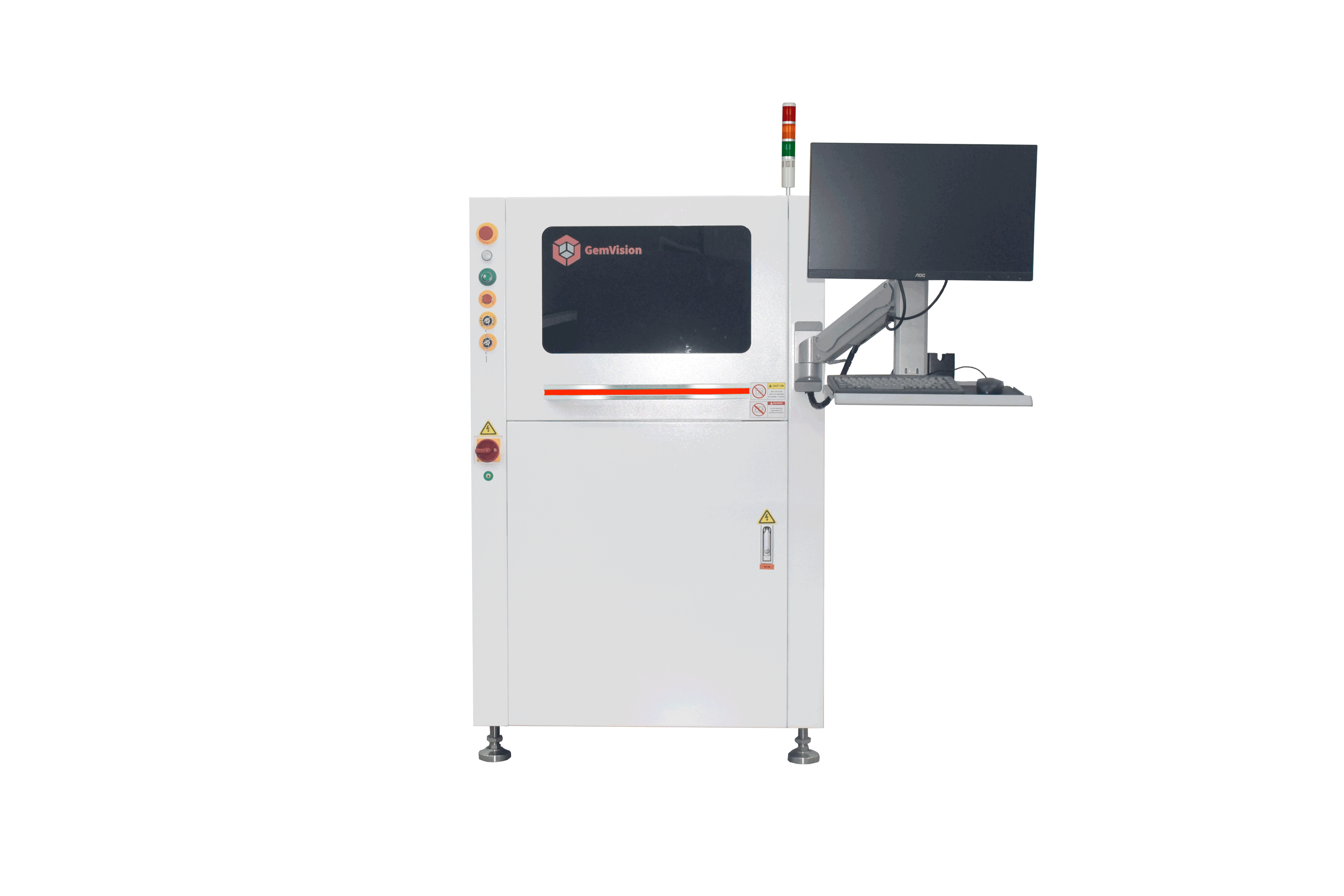
GA450
• Programmable Structured Grating PMP Imaging Technology [PATENTED]
• AI Intelligent Seamless “Jigsaw” Technology[PATENTED]
• AI Automatic Programming Technology [PATENTED]
• AI Algorithm Technology [PATENTED]
• Enhanced Super RGB Pro 2D Light Source [PATENTED]
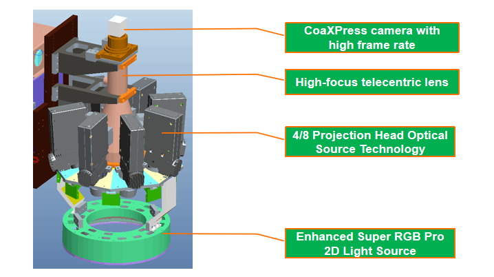
• 4/8 Projection Head Optical Source Technology [PATENTED]
• 15 Minutes AI Programming and 20~30 Minutes Fine Tuning Operation
• High-frame CXP Camera Solutions
• 3D+2D Ontology Localization Technology
• Self-developed MES Intelligent Manufacturing Access Capability
• Self-developed SPC Analysis Software & Closed-loop Control
Programmable structured grating PMP imaging technology (PSLM PMP) uses German PSLM components with international cutting-edge technology. [Ten-year free warranty]
Unique setup of the projection head optical source inspection.
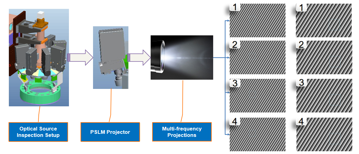
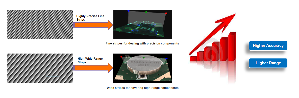
The equipment utilizes the programmable structured grating technology to intelligently switch between fine stripes and high wide-range stripes, driving phase shift errors towards zero. With no mechanical transmission components and no wear, it significantly enhances the equipment’s detection capabilities and scope of application.
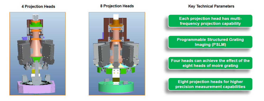
3D AOI uses optional 4+8 projection heads with PSLM multi-frequency projection capability to achieve the best inspection solution, covering all SMT/PTH/Semiconductor Applications.
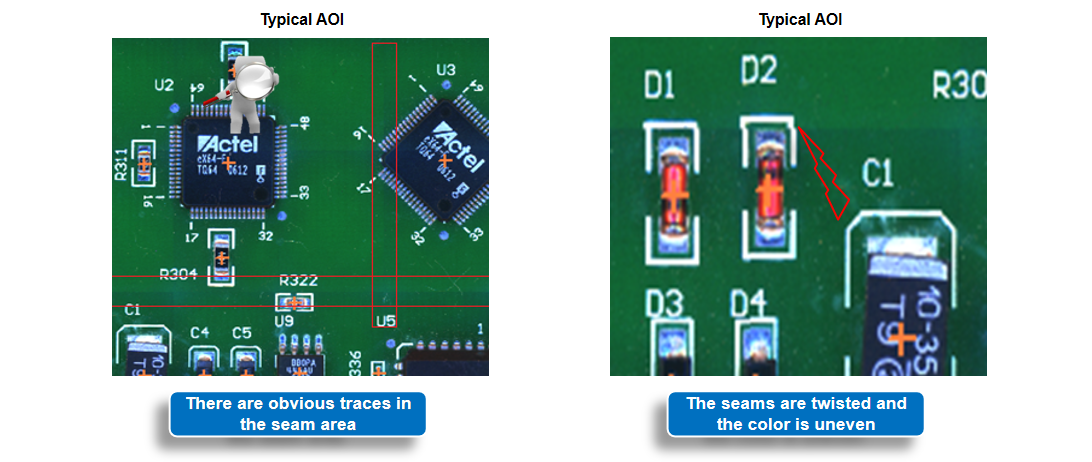
The problems of uneven images, uneven colors, and image distortion at the joints of FOV and FOV of typical AOI.
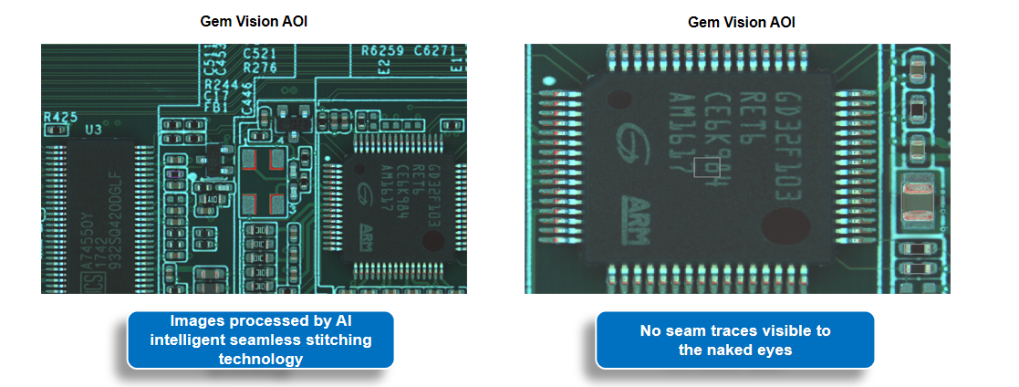
3D AOI uses innovative AI intelligent seamless “jigsaw” technology to achieve a level that is indistinguishable to the naked eyes. It perfectly solves the problems of unevenness, unevenness, distortion, etc. in the FOV image “jigsaw’ seams of traditional AOI. It improves the positioning accuracy of the detection frame and reduces program debugging time.
3D AOI uses intelligent program editing methods and template-based parameter setting methods to facilitate quick programming and debugging.
3D AOI uses AI algorithm to perform one of its detection capabilities to inspect IC pins height. The actual height of the pin is measured purely in 3D mode and compared with the standard threshold to confirm whether it is a fault.
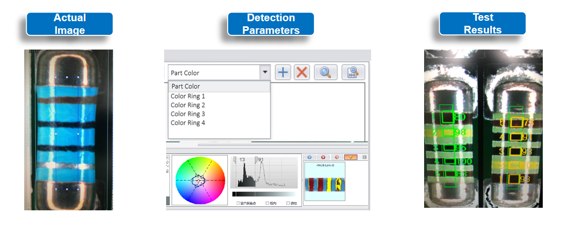
Another example of AI algorithm to perform resistor color code detection.
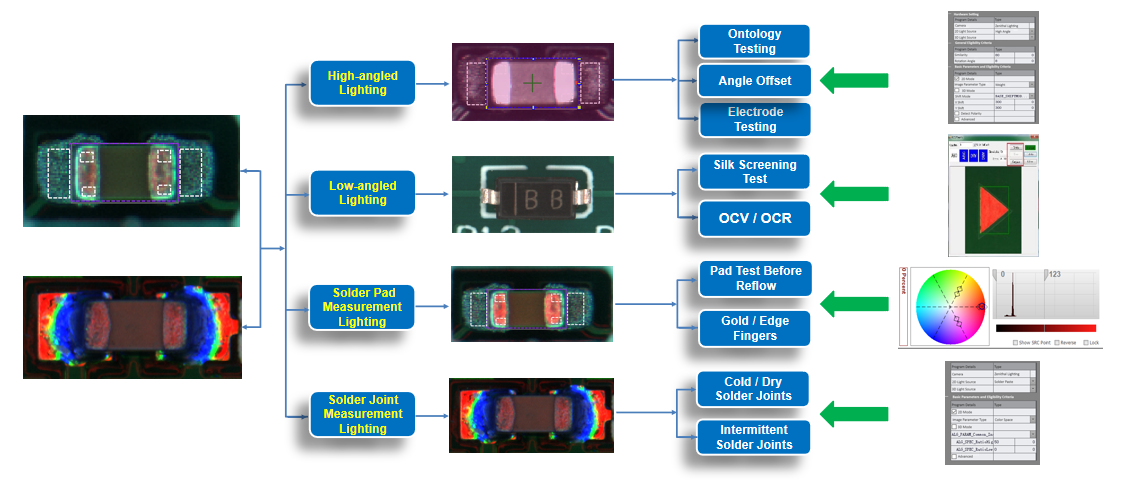
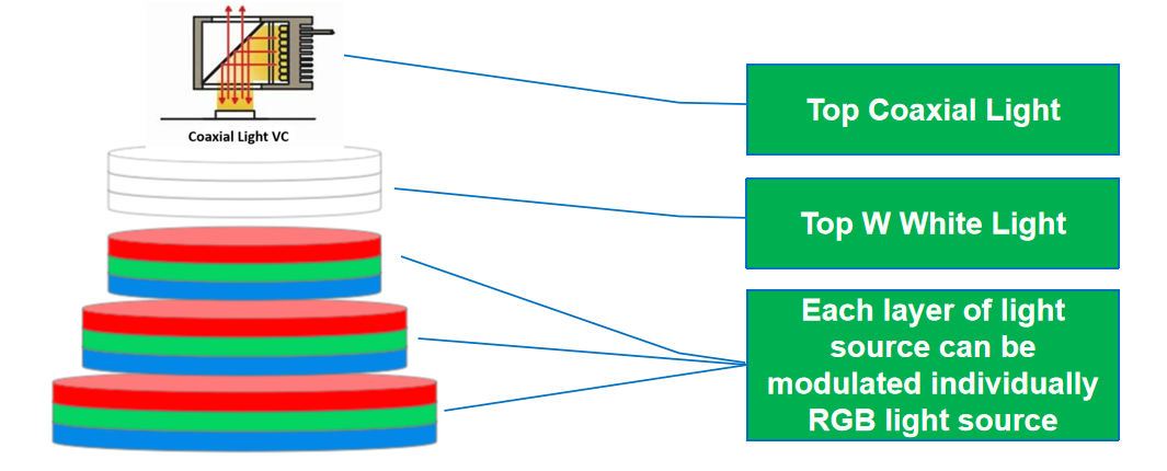
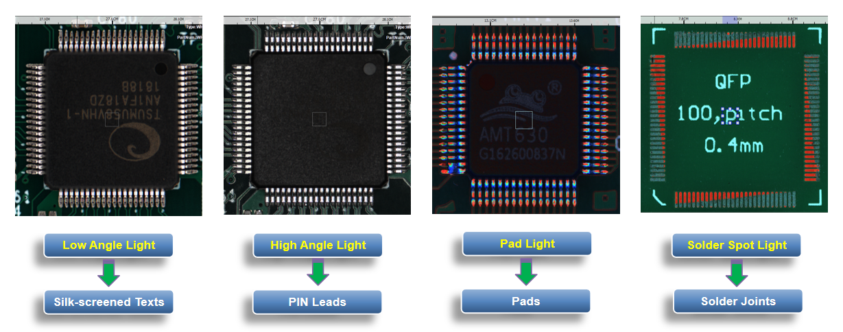
3D AOI adopts the self-developed enhanced multi-angle, multi-area, modulatable RGB+W+coaxial 2D light source design. It is suitable for the inspection of components, solder joints and text in various situations.
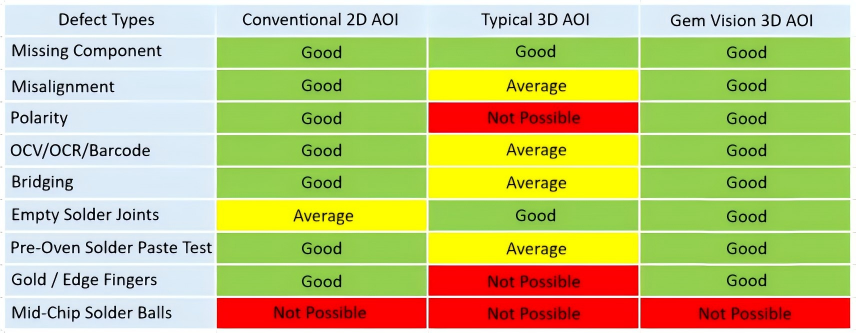
Gem Vision 3D AOI versus Other typical 3D AOI
| Technology Platform | Standard TYPE - C |
|---|---|
| Series | GA |
| Model | GA450 |
| Measurement Principle | Sine white projection PMP inspection |
| Measurements | Missing print, Offset, Rotation, Three-dimensional polarity, Upside down, OCV, Side standing, Tombstone, Poor soldering, etc. |
| Detection of Non-Performing Types | Solder tip, Solder volume percentage, Excessive solder, Insufficient solder, Bridge, Hole plugging, Solder filet, Pad contamination, etc. |
| Camera Pixel | 12M(19M, 21M optional) |
| Lens Resolution | 12M 12μm(12M 10μm/15μm optional; 21M 4μm~12μm optional) |
| XY Accuracy | XY (Resolution) ±10μm |
| Repeatability | height: ≤1μm (4 Sigma); volume/area:<1%(4 Sigma) |
| Gage R&R | <10% |
| Inspection Speed | 0.45sec/FOV~0.65sec/FOV(According to the actual configuration) |
| Quantity of Inspection Head | 4 (8 optional) |
| Mark-point Detection Time | '0.5sec/piece |
| Maximum Measuring Head | 10mm(25mm optional) |
| Maximum Measuring Height of PCB Warp | ±5mm |
| Minimum Pad Spacing | 100μm (Pad height of 150 μm as reference); 80μm/100μm/150μm/200μm (Determined by actual configuration) |
| Minimum element | 01005(03015/008004 optional) |
| Maximum height of element on PCB | 40mm |
| Maximum Measuring Height of PCB Warp | ±5mm |
| Minimum element | '01005 |
| Maximum Loading PCB Size(X*Y) | 450x460 (GA450) |
| Conveyor Setup | Front orbit (Back orbit optional) |
| PCB Transfer Direction | Left to right or Right to left |
| Conveyor Width Adjustment | Manual & Automatic |
| Engineering Statistics | SPC: Production Trend; Xbar-R Chart;Xbar-S Chart;CP&CPK;%Gage Repartability Data;AOI Daily/Weekly/Monthly Reports |
| Gerber & CAD Data Import | Support Gerber format (274x,274d), Manual teaching model, CAD X/Y import |
| Operating System Support | Windows 10 loT Enterprise (64 bit) |
| Equipment Dimension and Weight | W1000xD1174xH1550, 985Kg(GA450) |
| Optional | 1D/2D Barcode scanner, Badmark function, Three-point functions; Offline programming; Repair station |