


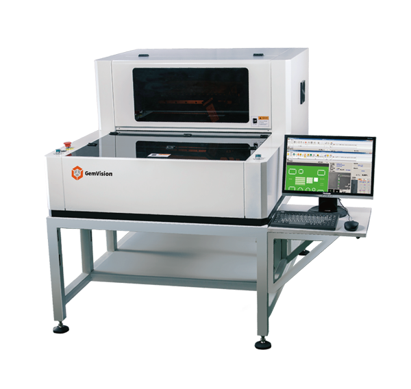
GT700
• Programmable Structured Grating PMP Imaging Technology [PATENTED]
• High and low exposure technology; D-Lighting [PATENTED]
• High-resolution lmage Processing System
• 5 Minutes AI Programming and One-Click Operation
• Step-and-Shot Imaging
• Servo Motor Drive
• SPC (Statistical Process Control) Process Control
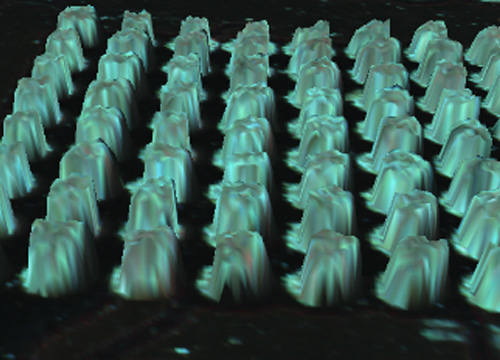
Phase modulation profilometry (PMP) is used to achieve 3D measurement of precision printed solder paste, which greatly improves the measurement accuracy while ensuring high-speed measurement.
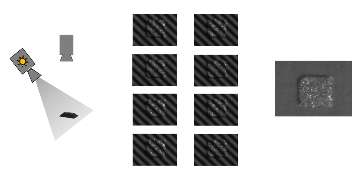
Phase modulation profilometry (PMP), also known as phase shift profilometry (PSP), is a method based on sinusoidal structure grating projection, discrete phase shift to obtain multiple deformed light field images, and then calculate the phase distribution according to the multi-step phase shift method, and finally use triangulation and other geometric methods to obtain high-precision height, area, and volume measurement results.
Programmable structured grating PMP imaging technology (PSLM PMP) uses German PSLM components with internationalcutting-edge technology. [Ten-year free warranty]
The object under inspection is sampled 8 times to ensure the high repeatability and accuracy of the equipment detection.
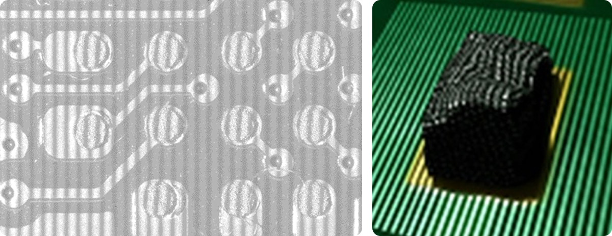
The white light source used by conventional SPI will not affect the color of the PCB, but for black (Dark PCB) and high brightness PCB boards (ceramic PCB), since the reflection degree of these two PCBs to the structured grating is different from that of ordinary PCBs, darker images will be displayed during imaging. Data accuracy is affected and false alarms will increase significantly.
The D-Lighting technology used by S-Tech uses 4 photos in a group of 8 sampled photos, using high exposure mode and low exposure mode respectively. In the setting software, you can choose black, normal, and high brightness options. Perfectly handle PCB boards with different reflectivity and different colors.
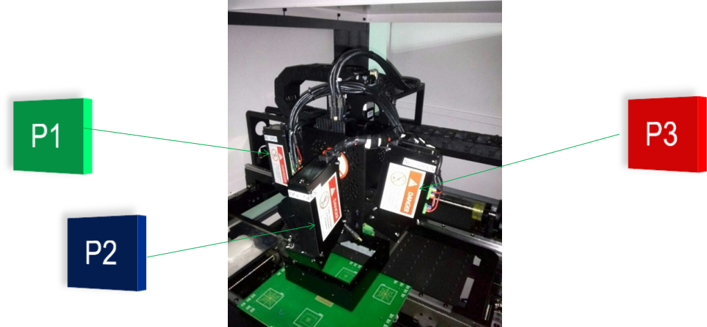
The unique Multi-Head optical source technology has obtained a national invention patent and uses 3 different colors of structured light to detect solder paste from different angles with an interval of 120°.
Flexible configuration to meet customer needs, optional single head, double head or multi-head.
Compared with the traditional white structured grating alternately taking pictures, Multi-Head can take pictures in multiple directions at the same time, which improves the detection speed.
| Technology Platform | |
|---|---|
| Series | GSO |
| Model | GT700 |
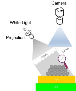
| Measurement Principle | 3D white light PSLM PMP (Programmable Spatial Light Modulation, Phase Measurement Profilometry) |
| Measurements | Volume, Area, Height, XY Offset, Shape |
| Detection of Non-Performing Types | Missing print, Insufficient solder, Excessive solder, Bridging, Offset, Mal-shapes, Surface contamination, etc. |
| Camera Pixel | 5M |
| Lens Resolution | 16μm (13μm optional) |
| Minimum element | 0201 (01005 optional) |
| Height Resolution | 0.37μm |
| FOV Size | 40*32mm(@5M 16μm) |
| XY Accuracy | XY direction:15μm |
| Repeatability | height: <1 μm(4 Sigma) ; volume/area: <1% (4 Sigma) |
| Gage R&R | <10% |
| Inspection Speed | 0.5sec/FOV |
| Quantity of Inspection Head | Single Head (Twin heads optional) |
| Mark-point Detection Time | 0.5 sec/piece |
| Maximum Measuring Height | ±550μm |
| Maximum Measuring Height of PCB Warp | ±5mm |
| Minimum Pad Spacing | 150μm (pad height of 150μm as the reference) |
| Smallest Measuring Size | rectangle:150μm;round:200μm |
| Maximum Loading PCB Size | X700 x Y600 mm |
| Fixed or Flexible Orbit Setting | Front orbit |
| Engineering Statistics | Histogram;Xbar-R Chart;Xbar-S Chart;CP&CPK;%Gage Repartability Data;SPI Daily/Weekly/Monthly Reports |
| Gerber & CAD Data Import | Support Gerber format (274x,274d), Manual teaching model, CAD X/Y, Part No.,Package Type input |
| Operating System Support | Windows 10 loT Enterprise (64 bit) |
| Equipment Dimension and Weight | 1500 x 1100 x 600mm;345KG |
| Optional | 1D / 2D Barcode scanner;UPS continuous power supply;workstation (Except GT700) |